The Quiet Shift: How AI Is Changing the Way PCBs Are Designed
For decades, PCB design has followed a familiar pattern.
An engineer sketches a schematic. Another spends days (or weeks) placing components and routing traces. Design reviews catch issues late. A respin follows. Everyone accepts this as “just how hardware works.”
That assumption is now being challenged.
Not by faster routers or slightly better DRCs — but by AI systems that treat PCB design as a solvable optimization and generation problem, not a purely manual craft.
This shift is still early, but it’s already changing how schematics are created, how layouts are produced, and how much human time is truly required.
Let’s look at what’s changing — and who is driving it.
From Drawing Boards to Describing Intent
Traditionally, PCB design has been an act of translation.
An engineer holds an idea in their head and manually translates it into:
- a schematic
- then a placement
- then thousands of routing decisions
Every step leaks intent. Every translation introduces risk.
AI changes this dynamic by shifting the engineer’s role upstream — from drawing to describing. Instead of focusing on how each trace is routed, engineers increasingly define what the board must achieve:
- functional blocks and interfaces
- physical and electrical constraints
- size, cost, layer count, and manufacturing limits
Once intent is explicit, software can help explore how best to realize it.

Where AI First Finds Its Footing
AI hasn’t taken over PCB design all at once. It has entered where friction is highest and mistakes are most expensive.
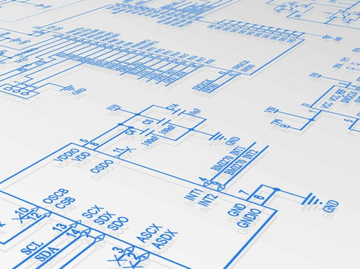
Schematic intelligence came first
Early gains appeared in schematic analysis and validation. AI systems learned to read schematics the way senior engineers do — spotting inconsistencies, missing components, and violations of datasheet constraints.
Instead of replacing engineers, these systems act like an always-on second set of eyes:
- catching errors early
- reducing back-and-forth during reviews
- preventing failures that only show up after fabrication
This quietly changed how teams think about “done” schematics.
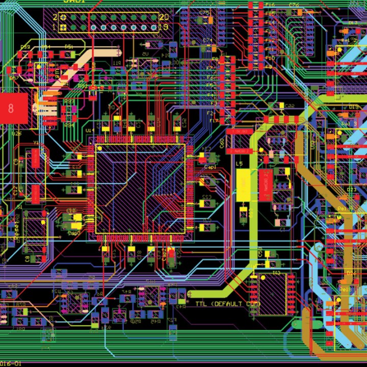
Layout became an optimization problem, not an art form
PCB layout was long treated as a craft — something learned through experience, intuition, and muscle memory.
AI reframed it differently.
Modern AI-driven layout tools treat PCB routing as:
- a constrained optimization problem
- a physics-aware search space
- a process that can produce multiple valid solutions, not just one
Instead of asking “How do I route this board?”, teams now ask:
Which of these layouts best balances performance, cost, and risk?
This subtle shift turns layout into a decision-making process rather than a manual bottleneck.
The Startups Pushing the Shift Forward
This transition is being driven less by incumbents and more by startups willing to rethink the workflow from first principles.
Pinscope — Teaching Software to Review Like an Engineer
Pinscope doesn’t try to design boards for you. Instead, it focuses on something far more practical: preventing mistakes before they become expensive.
By analyzing schematics against datasheets and design rules, Pinscope:
- identifies hidden risks
- flags violations early
- reduces dependence on late-stage reviews
It mirrors how senior engineers scan designs — but does it continuously and at scale.
Diode Computers — Treating PCBs as Generated Artifacts
Diode challenges a core assumption: that PCBs must be manually drawn at all.
Their approach treats PCB design as a code-driven process, where structured descriptions and constraints are translated into schematics and layouts. AI assists by:
- generating boards from specifications
- detecting logical and electrical errors
- exporting results to standard EDA tools
This blurs the boundary between hardware and software—and makes iteration dramatically faster.
quilter — Letting Physics Guide Automation
Quilter goes straight at the hardest problem: fully autonomous PCB layout that respects real-world physics.
Given a schematic and constraints, Quilter:
- generates complete board layouts
- evaluates signal integrity and manufacturability
- produces multiple design options in hours
The engineer’s job shifts from routing traces to choosing the best tradeoff.
That change alone reshapes timelines and team structure.
A Broader Pattern Emerges
These companies differ in approach, but they share a common belief:
PCB design does not need to be as manual as we’ve made it.
Other teams are reinforcing this idea:
- CircuitMind accelerates early schematic and BoM creation
- Flux embeds AI assistance directly into browser-based EDA tools
- DeepPCB applies reinforcement learning to routing decisions
- JITX treats boards as programmatically generated systems
Each attacks a different pain point, but all move design up the abstraction stack.
What Changes for Engineers and Teams
This shift doesn’t take engineers out of the loop — it moves them to a higher one.
Instead of spending large portions of their time pushing traces, fixing avoidable mistakes, or re-implementing patterns they’ve already solved dozens of times, engineers increasingly focus on what actually defines a good design. Their effort moves upstream: clarifying constraints, evaluating tradeoffs, and making system-level decisions that shape performance, cost, and reliability.
The practical outcome is significant. Smaller teams can now build more complex hardware, iteration cycles become shorter, and overall design quality improves. Not because engineers think less—but because they spend their thinking on the problems that matter most.
The Quiet Conclusion
AI is not replacing PCB designers. It is replacing the assumption that PCB design must be slow, fragile, and manual.
Years from now, fully hand-routing every board may feel like writing assembly code for a modern application — valuable in rare cases, unnecessary in most.
The shift isn’t loud. It isn’t sudden.
But it’s already happening — one schematic, one layout, one decision at a time.
Share this post: